| MOTHERBOARDS All The Ins and Outs of Your Vintage Computer's Drivetrain |
|||||||||||||||||||||||||||||||||||||||||||||||||||||||||||||||||||||||||||||||||||||||||||||||||||||||||||||||||||||||||||
|
If a CPU is like an "engine" then the "motherboard" is like the "Drivetrain", aka, transmission, tranxaxle, driveshafts, differentials, and all that fun stuff. It's basically what connects all of the other parts in your PC to make it "go". This is still just as true today, as it was back in the olden days of the eighties and nineties.
A motherboard is basically just a large circuit board covered to the brim in components that make your PC work. These motherboards match the form factor of the computer case you are intending to use: XT/Baby-AT, AT, ATX, mATX, SFX, NLX, or proprietary. Laptops are always a proprietary design. So here we are going to discuss EVERTHING having to do with the motherboard from a hardware sense, from what different areas of the board are dedicated to, what different generations of motherboard tend to be like, and where ports, connectors, and whatnot, are found.Motherboard Form Factors Motherboards come in form factors that are standardized, and in their own propreitary designs (some OEMS and Laptops). The form factor determines what kind of case(es) it will fit. Even proprietary designs might fit among multiple models of device. XT/BABY-AT FORM FACTOR MOTHERBOARDS - The XT/BABY AT form factor are boards up to roughly the size of a standard 8.5"x11" piece of paper in "portrait" orientation. They have five to nine holes for screws and possibly Stand-Offs in most cases, which slide into notches from the side of the motherboard mounting rails in the case and match up to one or two screw holes to fix it into place. These motherboards typically consist of eight expansion slots (less on later 386 and up boards in some cases), one large DIN-5 connector for the keyboard, at least pin headers for a internal speaker, and all the usual trimmings and fixings we'll talk about later. They only fit in XT, AT, and Baby AT Chassis, and only work with the P8 and P9 style power connectors. FULL SIZED AT MOTHERBOARDS - These somewhat rare and interesting motherboards were found during the 286 and early 386 era, with some examples as late as the mid 486 (DX2 era) stuff intended for use as a Server or high level workstation. These boards measure about 11"x11" or bigger, easily noticeable by the fact the keyboard jack appears to sit towards the middle (it's in the same spot as XT or Baby AT, just that much more real-estate was added to the board for components). The reason these boards had to be so big was VLSI (Very Large Scale Integration) was not common yet in the industry, so every function, from the RAM, to the memory controller, to the ISA Bus, required individual resistors, capacitors, transistors, diodes, driver ICs, multiplexers, AND/OR Gates, XOR gates, various CMOS chips....and all these take up way more space than when they were later consolidated into a single "die" and put onto 2-3 chips that take up about 1/10th the space...now known as a "Chipset". So the motherboards for the 286-486, in some cases, had to be frickin' huge! Full AT motherboards only fit into full AT chassis, and nothing else due to their size. LPX MOTHERBOARDS - LPX was a quasi-sub-standard based on the design of the IBM PS/2 Model 30, to allow for a low-profile, attractice case, that did not take up too much desk space, otherwise known as the "Pizza Box" pc design. These LPX MOtherboard, while generally and fairly interchangeable from one system to another, have one huge problem - the location, and particularly, the spacing of the central expansion slot for the riser card is not the same on all computers across all OEMs. Some compatible switchovers I know for a fact though would be NEC/Zenith Data Systems/Packard Bell, as Zenith, Packard Bell, and NEC were all sharing similar case designs and motherboards over a long period of time from about 1989-1995. IBM's systems in the PC-3xx and Aptiva series might also be interchangeable. ATX, mATX/SFX MOTHERBOARDS - The ATX standard turned the dimensions of the XT/Baby-AT Motherboard on it's side, reduced the slots by two, and added a rear "I/O Shield" that allowed for the same capacity for on-board devices that LPX had earlier (except in a far more standard design). mATX reduced the slots by 2 more to make the board smaller, and was a popular choice among OEMs at the time, while SFX was really just mATX with a different power supply. Of course there were a lot of proprietary designs (PC Jr, Tandy 1000, almost all laptops, some luggables, AT&T/Olivetti, and so on) which despite not fitting anything but the case they were designed for, still function in exactly the same way as the standard designs above.MOTHERBOARD ANATOMY BY GENERATION
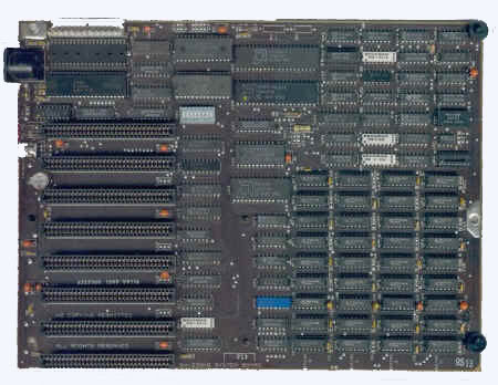 A vintage IBM Personal Computer XT Motherboard IBM XT CLASS MOTHERBOARDS - IBM XT Class Motherboards are almost always roughly 8.5"x11" in size, feature 8-9 holes for screws and possibly stand-offs. In the picture above, the bottom left corner is where the standard 8-bit ISA Slots, there's almost always eight of those. On teh lower right, are 4 banks of 9 DIP sockets for RAM. On the upper left corner we have a large DIN-5 connector for the keyboard, P8/P9 power input connectors, and the empty socket is for a Intel 8087 Math Co-Processor, with an Intel 8088 4.77MHz Processor chip beneath it. Next over are the IBM BIOS Chips and BASIC in ROM, with a eight pin DIP Switch header beneath it. This was how we configured PCs BEFORE the "CMOS Setup" became a thing. It's a pretty standard layout utilized across ALL XT class motherboards, save for maybe a few....see table below....*=Default Setting
RAM CONFIGURATION - XT BOARDS
VID CONFIGURATION - XT BOARDS
FLOPPY DRIVE CONFIGURATION - XT BOARDS
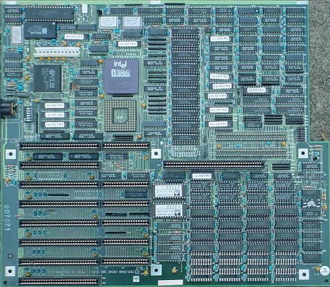
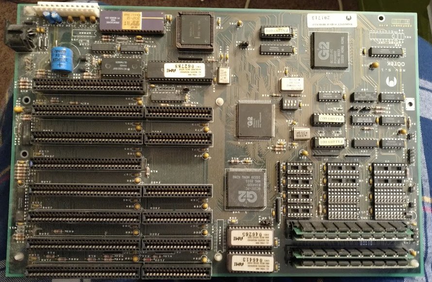 An Octek Rev 5.1 Motherboard out of a GEM Computer Products 286/10 system from 1989, which featured a full AT Case (LARGER & EARLIER) BABY AT (286) - As you can see, the dimensions of this Octek Revision 5.1 motherboard are similar to that of the actual true-blue IBM PC XT board above. That's beacuse they are basically the same motherboard in form factor, except this one is from a 1989 GEM Computer PRoducts 286/10 AT-clone system. So even if it has a full AT case, it does not mean it has a full AT motherboard. Anyway, as we can see now, the expansion slots on the lower left are now a mix of 8 and 16-bit ISA Slots, as this is an "AT Class" system (286). On the lower right, memory is now a mixed bag of 4 30-pin SIMM Sockets (hosting 4MB of RAM on this board, a whooping ton for a 286), and some DIP Sockets for DIP memory. Unfortunatley on this board, this memory cannot be mixed (some other boards allow that though). Again, the area in the upper right features P8/P9 for power (next to a row of Tantulums, 2 I replaced with electrolytics when they shorted/blew up), the infamous VARTA CMOS battery, an AMerican Megatrends Keyboard controller (to match the AMI BIOS found to the right of the expansion slots), and near that, the large purplish gray chip with the gold square is a IIT 802c87 Math Co-Processor at 12MHz, and next to that, in the PLCC Carrier, is a 10MHz Intel 80286 chip (overclocked of course :P), with it's clock crystal visible next to the keyboard controller chip. There are still DIP Switches on this board, which I'm not even sure whta they do, because the majority of what this motherboard does is controlled through the AMI BIOS CMOS firmware menus, accessible by pressing a special key combination on startup, and includes it's own diagnostic. The three large "G2" Chips are the "Chipset" that allow this board to work, basically they handle all the jobs originally carried out by discreet components that would require a larger motherboard, such as our next subject below....
 This one I stole from the Redhill.au website, a gianormous full-at DTK 386 motherboard from around 1990 or so, very late in the game for a full AT Motherboard. And as you can see, not a lot of VLSI either. Probably and earlier board re-released. FULL SIZED AT (286/386 era - 386 Shown) - Does anyone hear the beginning of Ghost's "Year Zero" when they see this monster? (Does the CPU Run on a MOnsterance clock?). Here it is, the myth, the legend, Full Sized AT. The original version of these boards would be the one found in the IBM PC AT 5170, but this is just as relevant as any. First off, note how far "in" the keyboard connector is - that's right about where Baby AT and XT Stop at their width, but this....hehe....this thing keeps on going another 3 or so inches. On the bottom left, again, ISA slots, including one 8-bit slot with a Memory Expansion slot at the end, a common practice on 386 DX motherboards at the time (and the Compaq Deskpro 386 they were cloning the ideas from also featured a proprietary 32-bit memory slot as SIMMS had not quite taken off yet). There's two DTK BIOS chips between the slots and the proprietary memory slot, and next to that, a very late case of 4 banks of 9 DIPS for RAM, plus 4 more SIP Sockets next to the proprietary memory connector, and above all that - GLUE LOGIC - ie discreet components that make everything work (hence this being full AT). Next to that is a row of L1 Cache chips (some 386 DX systems had L1 Cache). On the top right of course is P8/P9 power, the AT DIN jack, a VLSI chipset chep (apparently they missed the memo on what VLSI means on this board, lol), a row of 5 dip switches, and then the big 386 DX chip socket hosting a 25MHz 386 DX, and a empty socket for a 387, Fast Math, or Weitek math co-processor. Not a single square, bare inch of this board suprisingly. This is a bit atypical for a late 386, let's look at a 386SX Baby AT Motherboard for comparison....
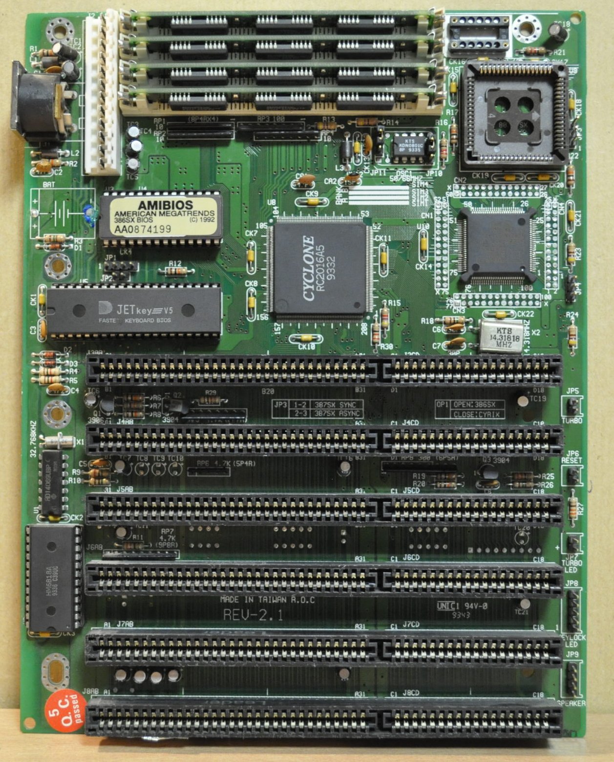 As "baby" as Baby AT Comes, this is a 386 SX motherboard from the later end of the 386's lifespan, probably around 1991-1992 or so. Look at how tiny this is compared to the 386 DX Behemoth above that's almost half the clockspeed! BABY AT (LATER) - 386 SX STYLE) - This is a pretty typical late 386-era/early 486-era baby AT motherboard for a 386 SX. It's so small it is HALF the length of a XT/Baby-AT style board from earlier, such as the GEM 286's board shown earlier. At the bottom we have six 16-bit ISA Slots, then above that is where the majority of the board's components are, from left to right: keyboard jack, keyboard controller chip (above ISA Slots), P8/P9 power connectors, American MegaTrends BIOS Chip, 4 30-pin SIMM Slots for up to 8MB of RAM, a "Cyclone" chipset chip that handles everything on the board (very similar to a modern PC actually), the surface-mount chip that looks like an "X" is the CPU - an AMD Am386 SX at 40MHz, and above that is a PLCC carrier for a 387SX math co-processor chip. There's also a spot for the Varta CMOS Battery (removed) shown toward the back.
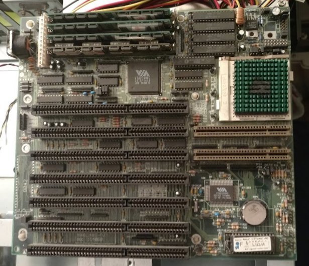 A First International Computer (FIC) 486-PVT Motherboard, this is the one in CreepingNet 486, back when that computer was being put together. A fine example of a mid-era 486 motherboard. MID-ERA 486 BABY-AT - You might be wondering why I'm posting so many pictures of so many boards, well, it's to familiarize you with the different styles, changes, and accomodations between generations and form factors. Here we have my own personal FIC 486-PVT, Socket 3 486 motherboard, the very one in CreepingNet 486 right now! On the bottom left of course are your explainsion slots, 7 in total, with the 2nd and 3rd from the top hosting the brown "backards PCI" VESA Local Bus extentions making them VLB slots, a bus largely unique to 486-era hardware. On the bottom right is a non-flashable Award BIOS Chip, a CR2302 CMOS Battery I installed myself (originally it had a tiny hearing aid battery, but it was silkscreened for the CR2302 on the board so I swapped), and a VIA BUS Controller chip. On the top left of course, is the big DIN-5 AT jack, 4 72-pin SIMM Sockets (with 64MB of RAM in them in the picture), some glue logic, jumpers for the L2 Cache chips which are just to the right of all that, a VIA Chipset, and then the entire top right of the board is dedicated to the Socket 3 486 CPU Socket, and setting it's voltage, bus speed, clock speed, and identifying it. In the picture I had a Intel 486 DX2-66 CPU installed with a Cyrix thermal-tape attached cooler, it now has active cooling and an AMD Am486 DX4-100 SV8T chip installed. Now, let's look at something Transitional and Pentium - and also something I owned at one point....
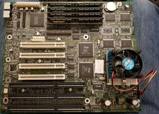 An Intel Desktop Board Socket 5 from 1995, from a 1995 Gateway 2000 P5-100 Desktop System I had TRANSITIONAL ERA BABY AT - SOCKET 5 - This motherboard is a transitional AT motherboard from a Gateway 2000 P5-100 system I gave to a friend as a going away present. It's a Socket 5 Pentium board with 64MB of RAM. Notice how different it looks from the FIC-486PVT board above. First off, we have two PS/2 ports instead of one DIN port for the keyboard, the second PS/2 port is for a mouse. Many during this time had a plug-in port that you could screw into a DB-9 hole on the back of the case. As you can see, we now have four (white) PCI Slots on the motherboard in addition to the three ISA Slots toward the bottom left. Again, similar to the FIC, it has 4 72-pin SIMM Slots, the CR2302 CMOS Battery is located on the top right above the 4 L2 Cache RAM Chips (IIRC it was 256 or 512K, maybe even 1MB), and the Socket 5 ZIF Socket with the cooler master cooler on it is home to a Intel Pentium 100MHz chip. Let's end the tirade of early AT with something really interesting....
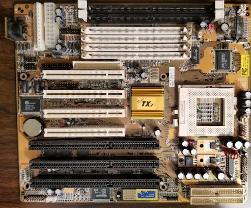 A late era circa 1997 PcChips Super Socket 7 board LAST OF THE ATs - SUPER SOCKET 7 - While AT Lasted into the PIII era, the last popular boards were in the 1997-1999 era of "Super Socket 7", which were motherboards with a "Socket 7" ZIF Socket on them, most of which could take any Intel Socket 5 CPU (75/90/100/133/200/233 with and without MMX Technology), as well as the new AMD K6 chips which were PII level processors that fit in a regular Socket 7 motherboard. On the bottom left we have the expansion slots, 3 ISA, 4 PCI of course, bottom right has the American Megatrends (AMI) BIOS chip, 2 40 pin 80-wire IDE Compatible sockets for up to 4 IDE devices, all the various capacitors and voltage control transistors for configuring the ZIF socket to the CPU's voltage/bus speed/clock speed. A CR2302 CMOS battery lives behind the first PCI slot. On the upper left we have 2 headers for Serial Ports, a Parellel Port, and Game Port, plus large DIN Keyboard port, another 5-pin provision for the PS/2 Mouse, and right beside the P8/P9 AT style power connector is another connector for an ATX power plug, then 2 DIMM Slots, 4 72 pin SIMM Slots, and the 34 pin floppy cable socket. Everything sits around a big golden cooler for the "TX" Chipset, and of course L2 Cache and glue logic on the upper right. It's basically a turnkey system, just add some RAM, a CPU, and then a modem or ethernet card, and you pretty much have a working system in a board. Just add PSU. Peripherals, Monitor, and Case and you've got a computer. A far cry from the XT board we started with where everything was on a card.
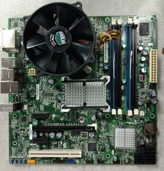 "BeigeBeast's Motherboard - an Intel DQ45CB, still quite a modern board (LG775) with a Core 2 Duo P8800 in it, but a fine example to cover all three birds with one stone. ATX/mATX - INTEL DQ45CB (2009) - While this is not a vintage board, it's a fine enough example of a ATX or Micro ATX motherboard to be exact to show both the changes, and how far we have come. Micro ATX could fit in a full ATX, Micro ATX, or SFX computer case just fine, and all three board types were made in Socket 7, Slot 1, Socket 375, Socket 478, and so on. This is basically a modern motherboard, which starts in 1998. First off, bottom left, we can see even in 2009 I got one standard PCI slot, along with a PCI Express slot in 8x and a 16x PCI-E Slot for a more powerful graphics card (an NVIDIA Quadro currently lives there). The intel chipset runs so fast it needs passive heatsinks on all of it just to cool itself off enough to function. There are 4 DDR2 DIMM Sockets on it for up to 16GB OF RAM, and a LGA 775 socket that can carry a Core 2 series chip of your choice. Behind the huge thermal unit there's the I/O Shield ports which includes 2x DVI, 1x HDMI, 1x external SATA, 4x USB 2.0, and I think Firewire IIRC. Older boards will also have a lot of the ports found on the PC Chips and others above, but this is a fine example of around the time they started dropping all the "legacy" items like PS/2, VGA, Serial, Parallel ports. Oh, and this has a sound-card as well on-board (AC97). Now, let's talk something...uh, "sub-standard" or "quasi-standard"....
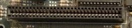
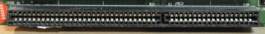
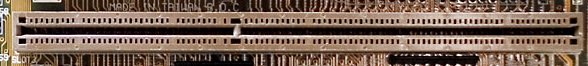
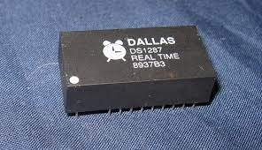
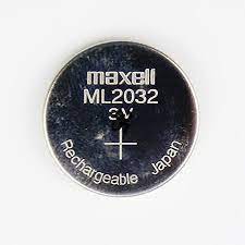
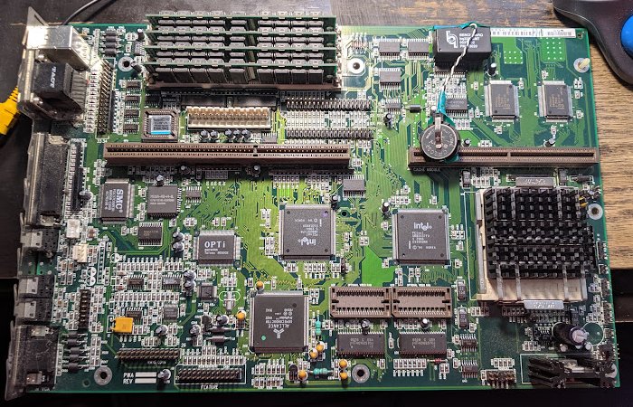 Socket 5 Motherboard from an NEC Ready 9522 LPX Tower from 1995 LPX - A QUASI/SEMI-STANDARD - "Low-Profile Extended" aka "LPX" is the psudeo-standard popular with OEM computer makers of the late 80's and early 1990's including (but not limited to): Acer, AST, Compaq, Dell, IBM, NEC, Packard Bell, and Zenith Data Systems - just to name a few. The first thing you'll notice is the entire left side is COVERED in ports. On a typical pre-Pentium LPX board this would have been - from top to bottom: 2x PS/2 (Mouse, Keyboard), Serial Ports (COM 1 and 2), Parallel, and VGA. IN the case of this NEC Ready 9522 though, this is PS2 Mouse and Keyboard stacked, COM1 and COM2 stacked ~ losing standardization already ~ then a Parallel Port, 2 Audio Ports for the OPTi Audio Chipset, and then a VGA Port for the on-board Alliance 1MB SVGA Graphics card. There's also a 15-pin header for a Game Port as well. The bottom left quadrant is all the electronics for audio and graphics, including 2 more PLCC carriers for an additional 1024K of VRAM on the lower right, as well as the Intel Chipset, Socket 5 CPU housing an Intel Pentium 100MHz chip, 4 dip switches for configuration, and even a port for active cooling on the board itself. The top left has 4 72 pin SIMM slots, housing 128MB of RAM, a pair of IDE Headers for the HDD/CD-ROM, P8/P9 standard AT/XT plugin for power, and then on the top right, we have 2 L2 Cache RAM chips, a "COAST" Socket (Cache on a STick) - which had a 256K module added to it - and then up at the top with a wire coming off to a CR2302 in a very popular mod, is the infamous Dallas Clock Chip - this is sometimes used intead of a regular CMOS battery. Instead it's an entire Real-Time Clock/Calendar on a single chip, and when the battery Dies, the system often won't retain it's settings nor boot. So one fix for that is to grind where 2 pins are not but are supposed to be, and wire in a harness for a CR2302 chip, and install the holder and the CR2302 button cell battery to have a working Dallas Clock again with a replaceable battery. But the star of the whole show - is the big brown slot near the middle - THAT is called the "Riser Card" slot (riser card not shown). The card basically looks like a expansion card with more expansion card sockets on it, in this case 1 PCI and 5 16-bit ISA. This is how they got those "Pizza Box" cases so short. However, in a touch of irony, this board came out of an LPX TOWER case - which tends to do the opposite of what LPX was invented to do - make the PC smaller. instead, it makes the tower wider to accomodate five slots (six actually) that if placed sideways like this would be in a desktop chassis, would save a lot of room. A GUIDE TO EXPANSION SLOTS Here's a quick guide to expansion slots on motherboards. Ever wondered was "16-bit ISA" or "PCI" means? Or what the port is for, then here's a quick table to let you know and see what they are.
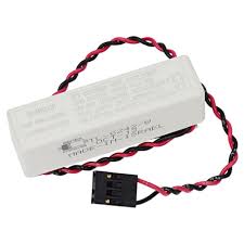
CMOS Batteries and You One of the most common things on motherboards on vintage PCs that you will have to deal with, is the CMOS battery, a little battery that may be either a coin cell, button cell, a Lithium Ion in a weird AA-like size, or a "Dallas Clock Chip" type. Anyway, this is a quick guide to these and their pros, cons, and caveats.
|